
URL
https://opencores.org/ocsvn/forth-cpu/forth-cpu/trunk
Subversion Repositories forth-cpu
[/] [forth-cpu/] [trunk/] [readme.md] - Rev 5
Compare with Previous | Blame | View Log
# Forth computing system| Project | Forth SoC written in VHDL || --------- | ------------------------- || Author | Richard James Howe || Copyright | 2013-2019 Richard Howe || License | MIT/LGPL || Email | howe.r.j.89@gmail.com |# IntroductionThis project implements a small stack computer tailored to executing Forthbased on the [J1][] CPU. The processor has been rewritten in [VHDL][] from[Verilog][], and extended slightly.The goals of the project are as follows:* Create a working version of [J1][] processor (called the H2).* Make a working toolchain for the processor.* Create a [FORTH][] for the processor which can take its input either from a[UART][] or a USB keyboard and a [VGA][] adapter.All three of which have been completed.The H2 processor, like the [J1][], is a stack based processor that executes aninstruction set especially suited for [FORTH][].The current target is the [Nexys3][] board, with a [Xilinx][] Spartan-6 XC6LX16-CS324[FPGA][], new boards will be targeted in the future as this board is reaching it'send of life. The [VHDL][] is written in a generic way, with hardware componentsbeing inferred instead of explicitly instantiated, this should make the codefairly portable, although the interfaces to the [Nexys3][] board components arespecific to the peripherals on that board.A video of the project in action, on the hardware, can be viewed here:And a lower quality version of the same video that should play automatically: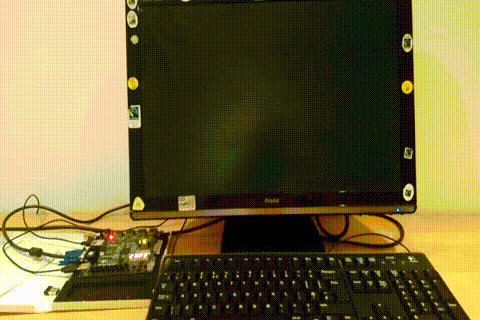The SoC can also be simulated with a simulator written in C, as shown below:The System Architecture is as follows: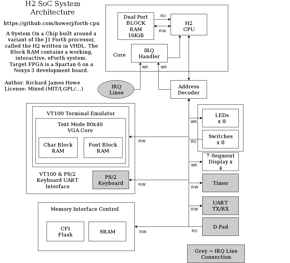# LicenseThe licenses used by the project are mixed and are on a per file basis. For mycode I use the [MIT][] license - so feel free to use it as you wish. The otherlicenses used are the [LGPL][] and the [Apache 2.0][] license, they are confinedto single modules so could be removed if you have some aversion to [LGPL][] code.# Target BoardThe only target board available at the moment is the [Nexys3][], this shouldchange in the future as the board is currently at it's End Of Life. The nextboards I am looking to support are it's successor, the Nexys 4, and the myStormBlackIce (<https://mystorm.uk/>). The myStorm board uses a completely opensource toolchain for synthesis, place and route and bit file generation.# Build and Running requirementsThe build has been tested under [Debian][] [Linux][], version 8.You will require:* [GCC][], or a suitable [C][] compiler capable of compiling [C99][]* [Make][]* [Xilinx ISE][] version 14.7* [GHDL][]* [GTKWave][]* [tcl][] version 8.6* Digilent Adept2 runtime and Digilent Adept2 utilities available at<http://store.digilentinc.com/digilent-adept-2-download-only/>* [freeglut][] (for the GUI simulator only)* [pandoc][] for building the documentation* [picocom][] (or an alternative terminal client)Hardware:* VGA Monitor, and cable (Optional)* USB Keyboard (Optional) (plugs into the Nexys3 USB to PS/2 bridge)* [Nexys3][] development board (if communication via UART only isdesired, the VGA Monitor and USB and Keyboard are not needed).* USB Cables![Xilinx ISE][] can (or could be) downloaded for free, but requiresregistration. ISE needs to be on your path:PATH=$PATH:/opt/Xilinx/14.7/ISE_DS/ISE/bin/lin64;PATH=$PATH:/opt/Xilinx/14.7/ISE_DS/ISE/lib/lin64;# Building and RunningTo make the [C][] based toolchain:make embed.hexTo make a bit file that can be flashed to the target board:make simulation synthesis implementation bitfileTo upload the bitfile to the target board:make uploadTo view the wave form generated by "make simulation":make viewerThe [C][] based CLI simulator can be invoked with:make runWhich will assemble the H2 Forth source file [embed.fth][], and run the assembledobject file under the H2 simulator with the debugger activated. A graphicalsimulator can be run with:make gui-runWhich requires [freeglut][] as well as a [C][] compiler.# Related ProjectsThe original [J1][] project is available at:* <http://www.excamera.com/sphinx/fpga-j1.html>This project targets the original [J1][] core and provides a eForthimplementation (written using [Gforth][] as for meta-compilation/crosscompilation to the [J1][] core). It also provides a simulator for the systemwritten in [C][].* <https://github.com/samawati/j1eforth>The eForth interpreter which the meta-compiler is built on can be found at:* <https://github.com/howerj/embed># ManualThe H2 processor and associated peripherals are now quite stable, however thesource is always the definitive guide as to how instructions and peripheralsbehave, as well as the register map.There are a few modifications to the [J1][] CPU which include:* New instructions* A CPU hold line which keeps the processor in the same state so long as it ishigh.* Interrupt Service Routines have been added.* Larger (adjustable at time of synthesis) return and data stacks### H2 CPUThe H2 CPU behaves very similarly to the [J1][] CPU, and the [J1 PDF][] can beread in order to better understand this processor. The processor is 16-bit withinstructions taking a single clock cycle. Most of the primitive Forth words canalso be executed in a single cycle as well, one notable exception is store ("!"),which is split into two instructions.The CPU has the following state within it:* A 64 deep return stack (up from 32 in the original [J1][])* A 65 deep variable stack (up from 33 in the original [J1][])* A program counter* An interrupt enable and interrupt request bit* An interrupt address register* Registers to delay and hold the latest IRQ and hold-line valuesLoads and stores into the block RAM that holds the H2 program discard thelowest bit, every other memory operation uses the lower bit (such as jumpsand loads and stores to Input/Output peripherals). This is so applications canuse the lowest bit for character operations when accessing the program RAM.The instruction set is decoded in the following manner:+---------------------------------------------------------------+| F | E | D | C | B | A | 9 | 8 | 7 | 6 | 5 | 4 | 3 | 2 | 1 | 0 |+---------------------------------------------------------------+| 1 | LITERAL VALUE |+---------------------------------------------------------------+| 0 | 0 | 0 | BRANCH TARGET ADDRESS |+---------------------------------------------------------------+| 0 | 0 | 1 | CONDITIONAL BRANCH TARGET ADDRESS |+---------------------------------------------------------------+| 0 | 1 | 0 | CALL TARGET ADDRESS |+---------------------------------------------------------------+| 0 | 1 | 1 | ALU OPERATION |T2N|T2R|N2A|R2P| RSTACK| DSTACK|+---------------------------------------------------------------+| F | E | D | C | B | A | 9 | 8 | 7 | 6 | 5 | 4 | 3 | 2 | 1 | 0 |+---------------------------------------------------------------+T : Top of data stackN : Next on data stackPC : Program CounterLITERAL VALUES : push a value onto the data stackCONDITIONAL : BRANCHS pop and test the TCALLS : PC+1 onto the return stackT2N : Move T to NT2R : Move T to top of return stackN2A : STORE T to memory location addressed by NR2P : Move top of return stack to PCRSTACK and DSTACK are signed values (twos compliment) that arethe stack delta (the amount to increment or decrement the stackby for their respective stacks: return and data)#### ALU operationsAll ALU operations replace T:| Value | Operation | Description ||-------|----------------|-----------------------|| 0 | T | Top of Stack || 1 | N | Copy T to N || 2 | T + N | Addition || 3 | T & N | Bitwise AND || 4 | T or N | Bitwise OR || 5 | T ^ N | Bitwise XOR || 6 | ~T | Bitwise Inversion || 7 | T = N | Equality test || 8 | N < T | Signed comparison || 9 | N >> T | Logical Right Shift || 10 | T - 1 | Decrement || 11 | R | Top of return stack || 12 | [T] | Load from address || 13 | N << T | Logical Left Shift || 14 | depth | Depth of stack || 15 | N u< T | Unsigned comparison || 16 | Set CPU State | Enable interrupts || 17 | Get CPU State | Are interrupts on? || 18 | rdepth | Depth of return stk || 19 | 0= | T == 0? || 20 | CPU ID | CPU Identifier || 21 | LITERAL | Internal Instruction |### Peripherals and registersRegisters marked prefixed with an 'o' are output registers, those with an 'i'prefix are input registers. Registers are divided into an input and outputsection of registers and the addresses of the input and output registers do notcorrespond to each other in all cases.The following peripherals have been implemented in the [VHDL][] SoC tointerface with devices on the [Nexys3][] board:* [VGA][] output device, text mode only, 80 by 40 characters from<http://www.javiervalcarce.eu/html/vhdl-vga80x40-en.html>. This hasbeen heavily modified from the original, which now implements most of a[VT100][] terminal emulator. This has two fonts available to it:- [Terminus][]/[KOI8-R][] (Default)- Latin [ISO-8859-15][] (Secondary Font) from<https://git.kernel.org/pub/scm/linux/kernel/git/legion/kbd.git>* [Timer][] in [timer.vhd][].* [UART][] (Rx/Tx) in [uart.vhd][].* [PS/2][] Keyboardfrom <https://eewiki.net/pages/viewpage.action?pageId=28279002>* [LED][] next to a bank of switches* A [7 Segment LED Display][] driver (a 7 segment display with a decimal point)The SoC also features a limited set of interrupts that can be enabled ordisabled.The output register map:| Register | Address | Description ||-------------|---------|---------------------------------|| oUart | 0x4000 | UART register || oVT100 | 0x4002 | VT100 Terminal Write || oLeds | 0x4004 | LED outputs || oTimerCtrl | 0x4006 | Timer control || oMemDout | 0x4008 | Memory Data Output || oMemControl | 0x400A | Memory Control / Hi Address || oMemAddrLow | 0x400C | Memory Lo Address || o7SegLED | 0x400E | 4 x LED 7 Segment display || oIrcMask | 0x4010 | CPU Interrupt Mask || oUartBaudTx | 0x4012 | UART Tx Baud Clock Setting || oUartBaudRx | 0x4014 | UART Rx Baud Clock Setting |The input registers:| Register | Address | Description ||-------------|---------|---------------------------------|| iUart | 0x4000 | UART register || iVT100 | 0x4002 | Terminal status & PS/2 Keyboard || iSwitches | 0x4004 | Buttons and switches || iTimerDin | 0x4006 | Current Timer Value || iMemDin | 0x4008 | Memory Data Input |The following description of the registers should be read in order and describehow the peripherals work as well.#### oUartA UART with a fixed baud rate and format (115200, 8 bits, 1 stop bit) ispresent on the SoC. The UART has a FIFO of depth 8 on both the RX and TXchannels. The control of the UART is split across oUart and iUart.To write a value to the UART assert TXWE along with putting the data in TXDO.The FIFO state can be analyzed by looking at the iUart register.To read a value from the UART: iUart can be checked to see if data is presentin the FIFO, if it is assert RXRE in the oUart register, on the next clockcycle the data will be present in the iUart register.The baud rate of the UART can be changed by rebuilding the VHDL project, bitlength, parity bits and stop bits can only be changed with modifications to[uart.vhd][]+-------------------------------------------------------------------------------+| 15 | 14 | 13 | 12 | 11 | 10 | 9 | 8 | 7 | 6 | 5 | 4 | 3 | 2 | 1 | 0 |+-------------------------------------------------------------------------------+| X | X |TXWE| X | X |RXRE| X | X | TXDO |+-------------------------------------------------------------------------------+TXWE: UART TX Write EnableRXRE: UART RX Read EnableTXDO: UART TX Data Output#### oVT100The VGA Text device emulates a terminal which the user can talk to by writingto the oVT100 register. It supports a subset of the [VT100][] terminalfunctionality. The interface behaves much like writing to a UART with the samebusy and control signals. The input is taken from a [PS/2][] keyboard availableon the board, this behaves like the RX mechanism of the UART.+-------------------------------------------------------------------------------+| 15 | 14 | 13 | 12 | 11 | 10 | 9 | 8 | 7 | 6 | 5 | 4 | 3 | 2 | 1 | 0 |+-------------------------------------------------------------------------------+| X | X |TXWE| X | X |RXRE| X | X | TXDO |+-------------------------------------------------------------------------------+TXWE: VT100 TX Write EnableRXRE: UART RX Read EnableTXDO: UART TX Data Output#### oLedsOn the [Nexys3][] board there is a bank of LEDs that are situated next to theswitches, these LEDs can be turned on (1) or off (0) by writing to LEDO. EachLED here corresponds to the switch it is next to.+-------------------------------------------------------------------------------+| 15 | 14 | 13 | 12 | 11 | 10 | 9 | 8 | 7 | 6 | 5 | 4 | 3 | 2 | 1 | 0 |+-------------------------------------------------------------------------------+| X | X | X | X | X | X | X | X | LEDO |+-------------------------------------------------------------------------------+LEDO: LED Output#### oTimerCtrlThe timer is controllable by the oTimerCtrl register, it is a 13-bit timerrunning at 100MHz, it can optionally generate interrupts and the current timersinternal count can be read back in with the iTimerDin register.The timer counts once the TE bit is asserted, once the timer reaches TCMP valueit wraps around and can optionally generate an interrupt by asserting INTE.This also toggles the Q and NQ lines that come out of the timer and are routedto pins on the board (see the constraints file [top.ucf][] for the pins).The timer can be reset by writing to RST.+-------------------------------------------------------------------------------+| 15 | 14 | 13 | 12 | 11 | 10 | 9 | 8 | 7 | 6 | 5 | 4 | 3 | 2 | 1 | 0 |+-------------------------------------------------------------------------------+| TE | RST|INTE| TCMP |+-------------------------------------------------------------------------------+TE: Timer EnableRST: Timer ResetINTE: Interrupt EnableTCMP: Timer Compare Value#### oIrcMaskThe H2 core has a mechanism for interrupts, interrupts have to be enabled ordisabled with an instruction. Each interrupt can be masked off with a bit inIMSK to enable that specific interrupt. A '1' in a bit of IMSK enables thatspecific interrupt, which will be delivered to the CPU if interrupts areenabled within it.+-------------------------------------------------------------------------------+| 15 | 14 | 13 | 12 | 11 | 10 | 9 | 8 | 7 | 6 | 5 | 4 | 3 | 2 | 1 | 0 |+-------------------------------------------------------------------------------+| X | X | X | X | X | X | X | X | IMSK |+-------------------------------------------------------------------------------+IMSK: Interrupt Mask#### oUartBaudTxThis register is used to set the baud and sample clock frequency fortransmission only.+-------------------------------------------------------------------------------+| 15 | 14 | 13 | 12 | 11 | 10 | 9 | 8 | 7 | 6 | 5 | 4 | 3 | 2 | 1 | 0 |+-------------------------------------------------------------------------------+| BTXC |+-------------------------------------------------------------------------------+BTXC: Baud Clock Settings#### oUartBaudRxThis register is used to set the baud and sample clock frequency forreception only.+-------------------------------------------------------------------------------+| 15 | 14 | 13 | 12 | 11 | 10 | 9 | 8 | 7 | 6 | 5 | 4 | 3 | 2 | 1 | 0 |+-------------------------------------------------------------------------------+| BRXC |+-------------------------------------------------------------------------------+BRXC: Baud Clock Settings#### oMemDoutData to be output to selected address when write enable (WE) issued inoMemControl.+-------------------------------------------------------------------------------+| 15 | 14 | 13 | 12 | 11 | 10 | 9 | 8 | 7 | 6 | 5 | 4 | 3 | 2 | 1 | 0 |+-------------------------------------------------------------------------------+| Data Ouput |+-------------------------------------------------------------------------------+#### oMemControlThis register contains the control registers for the onboard memory on the[Nexys3][] board. The board contains three memory devices, two non-volatilememory devices and a volatile RAM based device. The two devices accessible by asimple SRAM interface (one volatile M45W8MW16, one non-volatile - aNP8P128A13T1760E) are both accessible, the third is an SPI based memory device,NP5Q128A13ESFC0E) and is currently not accessible.+-------------------------------------------------------------------------------+| 15 | 14 | 13 | 12 | 11 | 10 | 9 | 8 | 7 | 6 | 5 | 4 | 3 | 2 | 1 | 0 |+-------------------------------------------------------------------------------+| OE | WE | RST|WAIT| RCS| FCS| Address Hi |+-------------------------------------------------------------------------------+OE: Output Enable - enable reading from current address into iMemDinWE: Write Enable - enable writing oMemDout into ram at current addressRST: Reset the Flash memory controllerRCS: RAM Chip Select, Enable Volatile MemoryFCS: Flash Chip Select, Enable Non-Volatile MemoryAddress Hi: High Bits of RAM addressOE and WE are mutually exclusive, if both are set then there is no effect.The memory controller is in active development, and the interface to it mightchange.#### oMemAddrLowThis is the lower address bits of the RAM.+-------------------------------------------------------------------------------+| 15 | 14 | 13 | 12 | 11 | 10 | 9 | 8 | 7 | 6 | 5 | 4 | 3 | 2 | 1 | 0 |+-------------------------------------------------------------------------------+| Address Lo |+-------------------------------------------------------------------------------+#### o7SegLEDOn the [Nexys3][] board there is a bank of 7 segment displays, with a decimalpoint (8-segment really), which can be used for numeric output. The LED segmentscannot be directly addressed. Instead the value stored in L8SD is mappedto a hexadecimal display value (or a BCD value, but this requires regenerationof the SoC and modification of a generic in the VHDL).The value '0' corresponds to a zero displayed on the LED segment, '15' to an'F', etcetera.There are 4 displays in a row.+-------------------------------------------------------------------------------+| 15 | 14 | 13 | 12 | 11 | 10 | 9 | 8 | 7 | 6 | 5 | 4 | 3 | 2 | 1 | 0 |+-------------------------------------------------------------------------------+| L7SD0 | L7SD1 | L7SD2 | L7SD3 |+-------------------------------------------------------------------------------+L7SD0: LED 7 Segment Display (leftmost display)L7SD1: LED 7 Segment DisplayL7SD2: LED 7 Segment DisplayL7SD3: LED 7 Segment Display (right most display)#### iUartThe iUart register works in conjunction with the oUart register. The status ofthe FIFO that buffers both transmission and reception of bytes is available inthe iUart register, as well as any received bytes.+-------------------------------------------------------------------------------+| 15 | 14 | 13 | 12 | 11 | 10 | 9 | 8 | 7 | 6 | 5 | 4 | 3 | 2 | 1 | 0 |+-------------------------------------------------------------------------------+| X | X | X |TFFL|TFEM| X |RFFL|RFEM| RXDI |+-------------------------------------------------------------------------------+TFFL: UART TX FIFO FullTFEM: UART TX FIFO EmptyRFFL: UART RX FIFO FullRFEM: UART RX FIFO EmptyRXDI: UART RX Data Input#### iVT100The iVT100 register works in conjunction with the oVT100 register. The status ofthe FIFO that buffers both transmission and reception of bytes is available inthe iVT100 register, as well as any received bytes. It works the same as theiUart/oUart registers.+-------------------------------------------------------------------------------+| 15 | 14 | 13 | 12 | 11 | 10 | 9 | 8 | 7 | 6 | 5 | 4 | 3 | 2 | 1 | 0 |+-------------------------------------------------------------------------------+| X | X | X |TFFL|TFEM| X |RFFL|RFEM| 0 | ACHR |+-------------------------------------------------------------------------------+TFFL: VGA VT100 TX FIFO FullTFEM: VGA VT100 TX FIFO EmptyRFFL: PS2 VT100 RX FIFO FullRFEM: PS2 VT100 RX FIFO EmptyACHR: New character available on PS2 Keyboard#### iTimerDinThis register contains the current value of the timers counter.+-------------------------------------------------------------------------------+| 15 | 14 | 13 | 12 | 11 | 10 | 9 | 8 | 7 | 6 | 5 | 4 | 3 | 2 | 1 | 0 |+-------------------------------------------------------------------------------+| X | X | X | TCNT |+-------------------------------------------------------------------------------+TCNT: Timer Counter Value#### iSwitchesiSwitches contains input lines from multiple sources. The buttons(BUP, BDWN, BLFT, BRGH, and BCNT) correspond to a [D-Pad][] on the [Nexys3][]board. The switches (TSWI) are the ones mentioned in oLeds, each have an LEDnext to them.The switches and the buttons are already debounced in hardware so they do nothave to be further processed once read in from these registers.+-------------------------------------------------------------------------------+| 15 | 14 | 13 | 12 | 11 | 10 | 9 | 8 | 7 | 6 | 5 | 4 | 3 | 2 | 1 | 0 |+-------------------------------------------------------------------------------+| X | X | X | BUP|BDWN|BLFT|BRGH|BCNT| TSWI |+-------------------------------------------------------------------------------+BUP: Button UpBDWN: Button DownBLFT: Button LeftBRGH: Button RightBCNT: Button CenterTSWI: Two Position Switches#### iMemDinMemory input, either from the SRAM or Flash, indexed by oMemControl andoMemAddrLow. When reading from flash this might actually be status informationor information from the query table.+-------------------------------------------------------------------------------+| 15 | 14 | 13 | 12 | 11 | 10 | 9 | 8 | 7 | 6 | 5 | 4 | 3 | 2 | 1 | 0 |+-------------------------------------------------------------------------------+| Data Input |+-------------------------------------------------------------------------------+### Interrupt Service RoutinesThe following interrupt service routines are defined:| Name | Number | Description ||-------------------|--------|-------------------------------|| isrNone | 0 | Not used || isrRxFifoNotEmpty | 1 | UART RX FIFO Is Not Empty || isrRxFifoFull | 2 | UART RX FIFI Is Full || isrTxFifoNotEmpty | 3 | UART TX FIFO Is Not Empty || isrTxFifoFull | 4 | UART TX FIFO Is Full || isrKbdNew | 5 | New PS/2 Keyboard Character || isrTimer | 6 | Timer Counter || isrDPadButton | 7 | Any D-Pad Button Change State |When an interrupt occurs, and interrupts are enabled within the processor, thena call to the location in memory is performed - the location is the same as theISR number. An ISR with a number of '4' will perform a call (not a jump) to thelocation '4' within memory, for example.Interrupts have a latency of at least 4-5 cycles before they are acted on, thereis a two to three cycle delay in the interrupt request handler, then the callto the ISR location in memory has to be done, then the call to the word thatimplements the ISR itself.If two interrupts occur at the same time they are processed from the lowestinterrupt number to the highest.Interrupts are lost when an interrupt with the same number occurs that has notbeen processed.# The ToolchainThe Disassembler and [C][] based simulator for the H2 is in a singleprogram (see [h2.c][]). This simulator complements the [VHDL][] test bench[tb.vhd][] and is not a replacement for it. The meta-compiler runs on top of aneForth interpreter and it contained within the files [embed.c][] and[embed.blk][]. The meta-compiler (Forth parlance for a cross-compiler) is aForth program which is used to create the eForth image that runs on the target.The toolchain is currently in flux, going forward there is liable to moreintegration between [h2.c][] and [embed.c][], along with changing the EmbedVirtual Machine into one that more closely resembles the H2 CPU with the longterm goal of creating a self hosting system.To build both, a [C][] compiler is needed, the build target "h2" will build theexecutable, h2, and "embed" will build the meta-compiler:make h2 embedAnd it can be run on the source file [embed.fth][] with the make target:make runThe make file is not needed:Linux:cc -std=c99 h2.c -o h2 # To build the h2 executablecc -std=c99 embed.c -o embed # To build the embed VM executable./embed embed.blk embed.hex embed.fth # Create the target eForth image./h2 -h # For a list of options./h2 -r embed.hex # Run the assembled fileWindows:gcc -std=c99 h2.c -o h2.exe # Builds the h2.exe executablegcc -std=c99 embed.c -o embed.exe # Builds the embed.exe executableembed.exe embed.blk embed.hex embed.fth # Create the target eForth iamgeh2.exe -h # For a list of optionsh2.exe -r embed.hex # Run the assembled fileA list of command line options available:- stop processing options, following arguments are files-h print a help message and exit-v increase logging level-d disassemble input files (default)-D full disassembly of input files-T Enter debug mode when running simulation-r run hex file-L # load symbol file-s # number of steps to run simulation (0 = forever)-n # specify NVRAM block file (default is nvram.blk)file* file to processThis program is released under the [MIT][] license, feel free to use it andmodify it as you please. With minimal modification it should be able toassemble programs for the original [J1][] core.## Meta-CompilerThe meta-compiler runs on top of the [embed][] virtual machine, it is a 16-bitvirtual machine that originally descended from the H2 CPU. The project includesa meta-compilation scheme that allows an eForth image to generate a new eForthimage with modifications. That system has been adapted for use with the H2,which replaced the cross compiler written in C, which allowed the first imagefor the H2 to be created.The meta-compiler is an ordinary Forth program, it is contained within[embed.fth][]. The meta-compiler Forth program is then used to build up aneForth image capable of running on the H2 target.For more information about meta-compilation in Forth, see:* <https://github.com/howerj/embed>* <https://github.com/howerj/embed/blob/master/embed.fth>* <http://www.ultratechnology.com/meta.html>## DisassemblerThe disassembler takes a text file containing the assembled program, whichconsists of 16-bit hexadecimal numbers. It then attempts to disassemble theinstructions. It can also be fed a symbols file which can be generated by theassembler and attempt to find the locations jumps and calls point to.The disassembler is used by a [tcl][] script called by [GTKwave][], itturns the instruction trace of the H2 from a series of numbers into theinstructions and branch destinations that they represent. This makes debuggingthe VHDL much easier.The purple trace shows the disassembled instructions.## SimulatorThe simulator in C implements the H2 core and most of the SoC. The IO for thesimulator is not cycle accurate, but can be used for running and debuggingprograms with results that are very similar to how the hardware behaves.This is much faster than rebuilding the bit file used to flash the [FPGA][].## DebuggerThe simulator also includes a debugger, which is designed to be similar to the[DEBUG.COM][] program available in [DOS][]. The debugger can be used todisassemble sections of memory, inspect the status of the peripherals and dumpsections of memory to the screen. It can also be used to set breakpoints,single step and run through the code until a breakpoint is hit.To run the debugger either a hex file or a source file must be given:# -T turns debugging mode on./h2 -T -r file.hex # Run simulatorBoth modes of operation can be augmented with a symbols file, which lists wherevariables, labels and functions are located with the assembled core.When the "-T" option is given debug mode will be entered before the simulationis executed. A prompt should appear and the command line should look like this:$ ./h2 -T -R h2.fthDebugger running, type 'h' for a list of commanddebug>Break points can be set either symbolically or by program location, the 'b'command is used to set breakpoints:Numbers can be entered in octal (prefix the number with '0'), hexadecimal(prefix with '0x') or in decimal. As an example, the following three debugcommands all set a breakpoint at the same location:debug> b 16debug> b 0x10debug> b 020'k' can be used to list the current break points that are set:debug> k0x0010This sets a breakpoint when the function "key?" is called:debug> b key?Functions and labels can both be halted on, this requires either asymbols file to be specified on the command line or assemble and runto be used on a source file, not a hex file. Symbol files can be usedon source or on hex files.To single step the 's' command can be given, although not much will happen iftracing is turned off (tracing is off by default). Tracing can be toggled on oroff with the 't' command:debug> sdebug> sdebug> ttrace ondebug> s0001: pc(089a) inst(4889) sp(0) rp(0) tos(0000) r(0000) call 889 initdebug> s0002: pc(0889) inst(807a) sp(0) rp(1) tos(0000) r(089b) 7adebug> s0003: pc(088a) inst(e004) sp(1) rp(1) tos(007a) r(089b) 6004It is advisable to turn tracing off when running issuing the 'c', or continue,command.The '.' command can be used to display the H2 cores internal state:debug> .Return Stack:0000: 0000 08aa 0883 017b 0000 031b 0000 ffb0 0000 02eb ffb5 0210 0167 01670167 01670010: 0000 0000 0000 0000 0000 0000 0000 0000 0000 0000 0000 0000 0000 00000000 0000Variable Stack:tos: 00000001: 0000 0000 0000 0001 0004 0005 0000 ffb0 0000 0000 0000 0000 0000 00000000 00000011: 0000 0000 0000 0000 0000 0000 0000 0000 0000 0000 0000 0000 0000 00000000 0000pc: 0538rp: 0001dp: 0000ie: falseAnd the 'p' command can be used to display the state of the simulatedperipherals:debug> pLEDS: 00VGA Cursor: 0005VGA Control: 007aTimer Control: 8032Timer: 001bIRC Mask: 0000UART Input: 6cLED 7seg: 0005Switches: 00LFSR: 40baWaiting: falseFor a complete list of commands, use the 'h' command.Other ways to enter debug mode include putting the ".break" assembler directiveinto the source code (this only works if the assemble and run command is usedon source files, not on hex files), and hitting the escape character when thesimulator is trying to read data via the simulated UART or PS/2 keyboard (theescape will still be passed onto the simulator, but it also activates debugmode).## Graphical simulatorA separate program can be compiled, tested under [Linux][] and [Windows][].This simulates the [Nexys3][] board peripherals that the SoC interfaces with,but provides a graphical environment, unlike the command line utility. It is easierto interact with the device and see what it is doing, but the debugging sessionsare a less controlled. It requires [free glut][].* VGA shown on screen.* UART or PS/2 input (selectable by pressing F11) comes from typing in the screen,and in the case of the UART this is buffered with a FIFO.* UART output gets written to a display box.* There are four 7-Segment displays as on the original board.* The switches and push buttons can take their input from either keyboard keysor from mouse clicks.* The LED indicators above the switches can be lit up.Below is an image of a running session in the GUI simulator:Building can be done withmake guiAnd running:make gui-runOr:./gui h2.hex (on Linux)gui.exe h2.hex (on Windows)The [Linux][] build should work when the development package for [free glut][]is installed on your system, the [Windows][] build may require changes to thebuild system and/or manual installation of the compiler, libraries and headers.The current key map is:Up Activate Up D-Pad Button, Release turns offDown Activate Down D-Pad Button, Release turns offLeft Activate Left D-Pad Button, Release turns offRight Activate Right D-Pad Button, Release turns offF1 - F8 Toggle Switch On/Off, F1 is left most, F8 Right MostF11 Toggle UART/PS2 Keyboard InputF12 Toggle Debugging InformationEscape Quit simulatorAll other keyboard keys are redirected to the UART or PS/2 Keyboard input.The Switches and D-Pad buttons can be clicked on to turn them on, the switchesturn on with left clicks and off with right clicks. The D-Pads buttons turn onwith a click on top of them and turn off with a key release anywhere on thescreen.# VHDL ComponentsThe VHDL components used in this system are designed to be reusable andportable across different toolchains and vendors. Hardware components, like blockRAM, are inferred and not explicitly instantiated. The components are also madeto be as generic as possible, with most having selectable widths. This would betaken to the extreme, but unfortunately many vendors still do not support theVHDL-2008 standard.| File | License | Author | Description || -------- | ---------- | --------------- | ----------------------------------- || util.vhd | MIT | Richard J Howe | A collection of generic components || h2.vhd | MIT | Richard J Howe | H2 Forth CPU Core || uart.vhd | MIT | Richard J Howe | UART TX/RX (Run time customizable) || vga.vhd | LGPL 3.0 | Javier V García | Text Mode VGA 80x40 Display || | | Richard J Howe | (and VT100 terminal emulator) || kbd.vhd | ??? | Scott Larson | PS/2 Keyboard |# eForth on the H2The pseudo Forth like language used as an assembler is described above, theapplication that actually runs on the Forth core is in itself a Forthinterpreter. This section describes the Forth interpreter that runs on H2 Core,it is contained within [embed.fth][].TODO:* Describe the Forth environment running on the H2 CPU.# Coding standardsThere are several languages used throughout this project, all of which areradically different from each other and require their own set of codingstandards and style guides.## VHDLCommon signal names:clk - The system clockrst - A reset signal for the modulewe - Write Enablere - Read Enabledi - Data Indin - Data Indo - Data Outdout - Data Outcontrol - Generally an input to a register, the documentationfor the module will need to be consulted to find outwhat each bit meanssignal_we - The write enable for 'signal'signal_i - This is an input signalsignal_o - This is an output signalGenerally the use of the "\_i" and "\_o" suffixes are not used, modules arekept short and names chosen so their meaning is obvious. This rule might berevisited once the project grows.Components should:* Be as generic as possible* Use an asynchronous reset* If a feature of a module can be made optional, by either ignoring outputsor setting inputs to sensible values, it should be.* Where possible use a function, it is easy enough to turn a genericcomponent into a module that can be synthesized but not the other way around.* Use "downto" not "to" when specify variable ranges.* Use assertions throughout the code with the correct severity level ('failure'for when something has seriously gone wrong or 'error' for debugging purposes)* Constrain types and generic parameters if possible, as an example, if a genericvalue should never be zero, use "positive" not "natural".* Try not to specify constants with fixed lengths where an expression using"others" can be used instead, for example:<!-- -->constant N: positive := 4;signal a: std_logic_vector(N - 1 downto 0) := (others => '1');Instead of:signal a: std_logic_vector(3 downto 0) := x"F";The style rules are as follows:* All words, including keywords, are to be in lower case. An underscorewill separate words in names.* Tabs are to be used to indent text, a tab spacing of 8 has been used whenmaking the VHDL code* Do not repeat the name of a entity, component, function or architecture,there is little point of repeating this, it just means when a unit has to berenamed it has to be done in two places instead of one.* The ":" in definitions of signals belongs next to the signal name, notsome arbitrary amount of spaces after it.* Group related signals.* Try to line up rows of signals* Trigger logic on the rising edge, and use the "rising\_edge" function not"clk'event and clk ='1'"* By and large, each warning produced by the synthesis tool should bejustified, and there should be very few warnings in the entire project if any.* Do not use inferred latches.* Load data from a file instead of generating VHDL files that contain the data,synthesis tools can handle impure VHDL functions that can read the initial data(for a ROM or block RAM as an example) from textual files.<!-- -->An example of the formatting guidelines, this describes a simple arbitrarywidth register:-- Lots of comments about what the unit does should go-- here. Describe the waveforms, states and use ASCII-- art where possible.library ieee, work;use ieee.std_logic_1164.all;use ieee.numeric_std.all; -- numeric_std not std_logic_arithentity reg is -- generic and port indented one tab, their parameters twogeneric (N: positive); -- Generic parameters make for a generic componentport (clk: in std_logic; -- standard signal namesrst: in std_logic; --we: in std_logic;di: in std_logic_vector(N - 1 downto 0);do: out std_logic_vector(N - 1 downto 0)); -- note the position of ");end entity; -- "end entity", not "end reg"architecture rtl of reg issignal r_c, r_n: std_logic_vector(N - 1 downto 0) := (others => '0');begindo <= r_c;process(rst, clk)beginif rst = '1' then -- asynchronous resetr_c <= (others => '0');elsif rising_edge(clk) then -- rising edge, not "clk'event and clk = '1'"r_c <= r_n;end if;end process;process(r_c, di, we)beginr_n <= r_c;if we = '1' thenr_n <= di;end if;end process;end; -- "end" or "end architecture"## CThere is quite a lot of [C][] code used within this project, used to make atool chain for the H2 core and to simulate the system.* Usage of assertions for any pre or post condition, or invariant, are encouraged.* Tabs are to be used instead of spaces, a tab width of 8 was used when codingthe C, if this causes any code to go off screen then there is a problem withthe code and not the tab length.* Generally the [K&R][] style is followed.* Line lengths should ideally be limited to 80 characters, but this isdefinitely not an enforced limit.* Where there are two or more data structures that must be kept in sync, with aone to one correspondence of elements, such as an enumeration and an array ofstrings that each enumeration maps onto, an [X-Macro][] should be used tokeep the data in sync and to initialize the enumeration and array of strings.* Try to use only portable constructs and isolate the constructs that are notportable.<!-- -->There is nothing too surprising about the [C][] code within here, so some ofthe exceptions should be dealt with.* Switch statements are formatted depending upon what the switch statement 'case'clauses look like, if they are a simple one liner such as an assignment or amapping then the entire statement should occupy only a single line, forexample:<!-- -->static const char *alu_op_to_string(uint16_t instruction) {/* notice also that the 'case' clauses are inline with the* switch selector */switch (ALU_OP(instruction)) {case ALU_OP_T: return "T";case ALU_OP_N: return "N";case ALU_OP_T_PLUS_N: return "T+N";case ALU_OP_T_AND_N: return "T&N";case ALU_OP_T_OR_N: return "T|N";case ALU_OP_T_XOR_N: return "T^N";case ALU_OP_T_INVERT: return "~T";case ALU_OP_T_EQUAL_N: return "N=T";case ALU_OP_N_LESS_T: return "T>N";case ALU_OP_N_RSHIFT_T: return "N>>T";case ALU_OP_T_DECREMENT: return "T-1";case ALU_OP_R: return "R";case ALU_OP_T_LOAD: return "[T]";case ALU_OP_N_LSHIFT_T: return "N<<T";case ALU_OP_DEPTH: return "depth";case ALU_OP_N_ULESS_T: return "Tu>N";case ALU_OP_ENABLE_INTERRUPTS: return "seti";case ALU_OP_INTERRUPTS_ENABLED: return "iset?";case ALU_OP_RDEPTH: return "rdepth";case ALU_OP_T_EQUAL_0: return "0=";case ALU_OP_CPU_ID: return "cpu-id";default: return "unknown";}}* Unnecessary braces are avoided:<!-- -->if (foo)bar();elsebaz();* "goto" can be used - it can be misused, but using it does not instantly makecode inscrutable contrary to popular belief.# To Do* Even better than using the [embed][] project directly, would be to port the[embed][] project so the meta-compiler runs directly on the hardware. Thesimulator could then be used to assemble new images, making the system (muchmore) self-hosting. Input/Output would be a problem, a possible solution is touse one of the UARTs for reading the meta-compiler and meta-compiled eForthprogram, and writing status/error messages. A second UART could be used todump the binary as a stream of hexadecimal numbers, the simulator couldredirect the second UART output to a file.* Create a cut down version of the project; remove nearly everything apart fromthe H2 Core, Block RAM and timer components. The interrupt handler could besimplified as well. The UART could be handed in the H2 Core* The GUI simulator could be written to be built against [SDL][], and includeproper textures for the buttons and displays, instead of the current simulatorwhich looks like an early 90s test application for OpenGL.* Prepare more documentation. Specifically about the eForth interpreter thatruns on the target and the online help stored within the non-volatile storageon the board.* An IDE for resetting/uploading the image to the target board and then sendinga text buffer to it would help in developing code for the platform.* A [Super Optimizer][] could be made for the H2.* More instructions can be combined* It might be possible to add a conditional exit instruction. Otherinstructions which would be useful are: Add with Carry, Bit Count, LeadingZeroes Count, Sign Extend, Arithmetic Right Shift, Rotate Left/Right, ...* Add notes about picocom, and setting up the hardware:<!-- -->picocom --omap delbs -b 115200 -e b /dev/ttyUSB1# Resources* <https://nanode0000.wordpress.com/2017/04/08/exploring-the-j1-instruction-set-and-architecture/>* <https://www.fpgarelated.com/showarticle/790.php>* <https://opencores.org/>* <https://en.wikipedia.org/wiki/Peephole_optimization>* <https://en.wikipedia.org/wiki/Superoptimization>* <https://github.com/samawati/j1eforth>* <https://github.com/jamesbowman/j1>* <http://sovietov.com/app/forthwiz.html>[j1eforth]: https://github.com/samawati/j1eforth[javascript]: https://www.javascript.com/[emscripten]: https://github.com/kripken/emscripten[DEBUG.COM]: https://en.wikipedia.org/wiki/Debug_%28command%29[DOS]: https://en.wikipedia.org/wiki/DOS[h2.c]: h2.c[embed.fth]: embed.fth[embed.c]: embed.c[embed.blk]: embed.blk[tb.vhd]: tb.vhd[uart.vhd]: uart.vhd[timer.vhd]: timer.vhd[top.ucf]: top.ucf[font.bin]: font.bin[text.bin]: text.bin[J1]: http://www.excamera.com/sphinx/fpga-j1.html[J1 PDF]: http://excamera.com/files/j1.pdf[PL/0]: https://github.com/howerj/pl0[libforth]: https://github.com/howerj/libforth/[MIT]: https://en.wikipedia.org/wiki/MIT_License[LGPL]: https://www.gnu.org/licenses/lgpl-3.0.en.html[VHDL]: https://en.wikipedia.org/wiki/VHDL[Verilog]: https://en.wikipedia.org/wiki/Verilog[UART]: https://en.wikipedia.org/wiki/Universal_asynchronous_receiver/transmitter[FORTH]: https://en.wikipedia.org/wiki/Forth_%28programming_language%29[Nexys3]: http://store.digilentinc.com/nexys-3-spartan-6-fpga-trainer-board-limited-time-see-nexys4-ddr/[Make]: https://en.wikipedia.org/wiki/Make_%28software%29[C]: https://en.wikipedia.org/wiki/C_%28programming_language%29[Debian]: https://en.wikipedia.org/wiki/Debian[Linux]: https://en.wikipedia.org/wiki/Linux[GCC]: https://en.wikipedia.org/wiki/GNU_Compiler_Collection[Xilinx ISE]: https://www.xilinx.com/products/design-tools/ise-design-suite.html[Xilinx]: https://www.xilinx.com[GHDL]: http://ghdl.free.fr/[GTKWave]: http://gtkwave.sourceforge.net/[C99]: https://en.wikipedia.org/wiki/C99[tcl]: https://en.wikipedia.org/wiki/Tcl[Wishbone interface]: https://en.wikipedia.org/wiki/Wishbone_%28computer_bus%29[D-Pad]: https://en.wikipedia.org/wiki/D-pad[FIFO]: https://en.wikipedia.org/wiki/FIFO_%28computing_and_electronics%29[VGA]: https://en.wikipedia.org/wiki/Video_Graphics_Array[PS/2]: https://en.wikipedia.org/wiki/PS/2_port[LED]: https://en.wikipedia.org/wiki/Light-emitting_diode[7 Segment LED Display]: https://en.wikipedia.org/wiki/Seven-segment_display[ISO 8859-1 (Latin-1)]: https://cs.stanford.edu/people/miles/iso8859.html[Spartan 6]: https://www.xilinx.com/products/silicon-devices/fpga/spartan-6.html[FPGA]: https://en.wikipedia.org/wiki/Field-programmable_gate_array[ASCII]: https://en.wikipedia.org/wiki/ASCII[free glut]: http://freeglut.sourceforge.net/[pthreads]: https://en.wikipedia.org/wiki/POSIX_Threads[LFSR]: https://en.wikipedia.org/wiki/Linear-feedback_shift_register[freeglut]: http://freeglut.sourceforge.net/[EBNF]: https://en.wikipedia.org/wiki/Extended_Backus%E2%80%93Naur_form[K&R]: https://en.wikipedia.org/wiki/Indent_style#K.26R[X-Macro]: https://en.wikipedia.org/wiki/X_Macro[Windows]: https://en.wikipedia.org/wiki/Windows_7[pandoc]: https://pandoc.org[picocom]: https://github.com/npat-efault/picocom[Gforth]: https://www.gnu.org/software/gforth/[opencores]: https://opencores.org[VT100]: https://en.wikipedia.org/wiki/VT100[embed]: https://github.com/howerj/embed[SDL]: https://www.libsdl.org/[Apache 2.0]: https://www.apache.org/licenses/LICENSE-2.0.html[KOI8-R]: https://en.wikipedia.org/wiki/KOI8-R[Terminus]: http://terminus-font.sourceforge.net/[ISO-8859-15]: https://en.wikipedia.org/wiki/ISO/IEC_8859-15[Super Optimizer]: https://en.wikipedia.org/wiki/Superoptimization<!--https://www.w3schools.com/css/css_table.asphttp://adis.ca/entry/2011/pretty-code-block-in-css/https://www.w3.org/Style/Examples/007/center.en.htmlhttps://css-tricks.com/centering-css-complete-guide/--><!----><style type="text/css">body{margin:40px auto;max-width:850px;line-height:1.6;font-size:16px;color:#444;padding:0 10px}h1,h2,h3{line-height:1.2}table {width: 100%; border-collapse: collapse;}table, th, td{border: 1px solid black;}code { color: #091992; } </style>