ag_6502 soft core with phase-level accuracy
Project maintainers
Details
Created: Mar 13, 2012
Updated: Jul 31, 2012
SVN Updated: Jun 11, 2012
SVN: Browse
Latest version: download (might take a bit to start...)
Statistics: View
Bugs: 1 reported / 1 solved
Other project properties
Language:Verilog
Development status:Beta
Additional info:Design done, FPGA proven
WishBone compliant: No
WishBone version: n/a
License: GPL
Description
The main features of ag_6502 implementation:
* It provides not only clock-level compatibility, but phase-level compatibility too. Thus it may be possible to connect simulated 6502 instead of the original one. Source code includes two possibilities to simulate two-phase clocking: by the use of external phi1 and phi2 clock generators and by the simulation of the phase shift using higher frequency source (I used standard 50 MHz clock generator to simulate phases phi1 and phi2 in my test project).
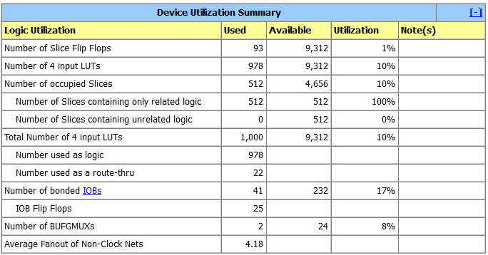
* It requires a relatively small amount of FPGA logic, for example in Xilinx Spartan-3E:
Flop Flops: 93
LUTs: 978
Slices: 512
* In the current implementation the following CPU commands are implemented:
- All legitimate commands including ADC/SBC in decimal mode (not all illegal features are fully implemented, such as N, Z flags usage in the decimal mode);
- All KILLs;
- All NOPs including their "addressing modes";
- All LAX illegal commands;
- For all other known illegal commands, only fetch and addressing parts are implemented. No real operations are performed, and timings for these commands may be not accurate.
* All input signals are implemented, including RST, IRQ/NMI interrupts, RDY line and even SO pin.
* Maximum tested frequency for Spartan 3E: 10 MHz (10 times faster than original 6502).
"Genstates" Compiler Information
For the development of this core I designed and implemented a simple programming language with optimizing compiler ("genstates") producing verilog source (see states.v in the source tree). The main idea of this approach is to minimize required amount of registers replacing them with wires and assigns in Verilog, like it was in MOS 6502. The process of the execution of processor command is described by a sequence of arbitrary mnemonical commands divided by two clock phases and by execution stages (0-fetch etc). On the first phase (phi1) processor drives address bus, R/W line and data output bus (for write). Also it multiplexes internal buses and sets the necessary modes for the following execution. On the second phase (phi2) processor reads data input bus (for read) and performs all internal operations like it was in it's original prototype. The compiler transforms all mnemonical commands into a list of assigns where single command will be just a wire which will be assigned to 1 if in the current moment this command should be executed, and to 0 if not. The real execution of this commands is performed by a main hand-written code. Example of mnemonical program:
#09:    % ORA #IMM
(0:1    AB <= PC
(0:2    PC <= PC + 1
(1:1    AB <= PC
        SB = DB
        ALU_A = AC
        ALU_B = SB
        ALU_OP = ORA
(1:2    PC <= PC + 1
        AC <= RES
        N,Z <= RES
        T <= 0
Example of some of generated wires (after automatic optimization):
//    action: DB <= ALU:
    assign E_DB__ALU = ({L[0],L[1],L[2],L[3],L[4],L[6],L[7],L[8],L[9],L[10]} == 10'b0110011110) ||
(({L[0],L[1],L[2],L[6],L[7],L[10]} == 6'b011111) && ((!L[9] && ((!L[3] && (({L[4],L[8]} == 2'b00) || L[4])) || (L[3] &&
(({L[4],L[8]} == 2'b00) || L[8])))) || ({L[3],L[4],L[8],L[9]} == 4'b1101)));

//    action: DB <= PCH:
    assign E_DB__PCH = ({L[0],L[1],L[2],L[3],L[4],L[5],L[6],L[7],L[8],L[9],L[10]} == 11'b00000000010) ||
({L[0],L[1],L[2],L[3],L[4],L[5],L[6],L[7],L[8],L[9],L[10]} == 11'b00000100110);

//    action: PCL <= EAL:
    assign E_PCL__EAL = ({L[0],L[1],L[2],L[3],L[4],L[5],L[6],L[7],L[8],L[9],L[10]} == 11'b00000100101);
In the example above the L vector is just a selector made of 8-bit opcode and 3-bit time counter:
wire[10:0] L = {T, IR_eff};
Example of some action handlers:
    assign SB = A_SB_DB? db_in:
                    A_SB_AC? AC:
                    A_SB_X? X:
                    A_SB_Y? Y:
                    A_SB_S? S:
                    A_SB_P? P:
                    A_SB_ALU? ALU:
                    A_SB_0? 8'b0:
                    A_SB_PCH? PCH:
                    A_SB_PCL? PCL:
                    8'bX;
    assign ALU_B = A_ALU_B_SB? SB:
                    A_ALU_B_NOTSB? ~SB:
                    8'bX;
    always @(posedge phi_1) begin
        if (E_AB__PC) ab <= PC;
        else if (E_AB__EA) ab <= EA;
        else if (E_AB__S) ab <= {8'b1, S};
        ...
Thus it is possible to easily extend functionality of this model without the need of boring bit-level programming, because main code deals only with relatively high-level objects described by auto-generated wires. Also it is possible to implement any other processor core with this approach, because the description language is completely abstract.